Description
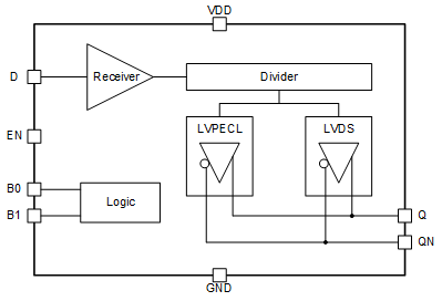
The AZS10 is a configurable LVPECL, LVDS buffer & translator IC that is optimized for ultra-low phase noise and additive jitter operating at 2.5V & 3.3V nominal supply voltages. It is particularly useful in converting crystal or SAW based oscillators into LVPECL and LVDS outputs for signals up to 1.5GHz. The AZS10 is a configurable IC design capable of providing LVPECL or LVDS outputs, ÷1 or ÷2 function, and active high or active low enable selection that provide designers with a single high performance IC buffer/translator solution that is extremely compact and flexible.
Recommended for new designs
Block Diagram

- • 38fs additive jitter
- • -167dBc/Hz LVPECL phase noise floor
- • Up to 1.5GHz operation
- • Internal divider
- • 2.5 – 3.3V analog supply
- • Extended Temp Range: -40°C to 125°C
- • Crystal or SAW Oscillators
- • Clock references and drivers
- • Signal conversion
- • Clock fanout
Order Numbers
| Part Number | Package | Dimensions | Quantity | MSL Rating | Leadframe |
|---|---|---|---|---|---|
| AZS10QGR1 | SON8 | 1.5mm x 1.0mm | 1000 | 1 | NiPdAu |
| AZS10TGR1 | MSOP8 | 0.12in x 0.12in | 1000 | 1 | NiPdAu |

